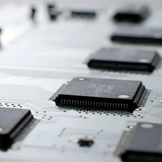

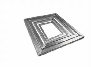
When surface mount material (SMD) typesetting process is desired for printed circuit boards, sieve is an auxiliary material that allows the cream solder to be transferred to the printed circuit boards correctly. The main purpose of using a sieve is to shorten the manufacturing time and ensure faster manufacture. There are two main types as cream solder sieve and glue sieve. The most commonly used type of sieve is laser-cut cream solder sieve. The sieves can be framed or as sheets. Framed screens are glued to the frame with special adhesives on stretched silk and are used as stretched in this way with a long service life. Today, there are also automatic frame systems that can replace the internal steel sieve.
Types of Cream Solder Sieves
Steel Sieve (Laser Cutting):
It is the sieve through which the areas are opened using a laser. It can be produced as framed or sheet. The advantages and disadvantages compared to other sieves are as follows.
- The inside of the cut holes are smoother and flatter.
- By making precise cuts, the correct result can be achieved.
- The printing circuit board soldering quality is high.
- It can be used for BGA and QFP applications without any issues.
- Its service life is longer than other sieves. The overall life is 60,000 prints.
- It is costly due to the laser cutting costs.
Phosphor Bronze (Etching):
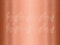
Phosphor is produced from bronze material. The areas are opened with chemical etching. Laser cutting is cheaper than steel sieve, but laser cutting has less precision than that of steel sieve. It is mainly used to reduce the costs and create a temporary solution in manufacturing cases with low quantity and without sensitivity. It is short-lived, and not resistant to rusting and deterioration.
Glue (Sticky) Sieve:
It is a sieve that allows surface mounting materials (SMD) to hold onto the plate through their bodies. FR4 plates are formed by drilling round holes on CNC machines. Usually, the holes drilled are not under 0.5 mm. Steel laser cutting sieve can be preferred for glue sieve. Here, steel with a thickness of 200um is usually used and laser cuts are made in a round slot shape.
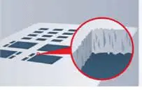
What is Electro Polishing?
It is also known as electrochemical deburring. With this method, small burrs are removed and the surface quality is improved. The holes drilled on the sieve can be reduced to below 1um. This method is important for the high-quality installation of BGA and QFP cases with a leg interval of less than 0.5 mm.
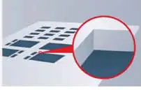
Sieve Fiducial Etching (Fiducial Marks)
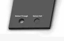
The basic signs used as a reference for machines in PCB and sieve matching are fiducial ones. They are basically round in shape. There are also different types. This fiducial can be made on a single surface with 30-50% etching. If the fiducial mark is requested on 2 surfaces of the sieve, 30% on both surfaces can be opened.
Sieve Dimensions and Thicknesses
Sieves are manufactured in different thicknesses and sizes according to the types of materials in the project where they will be used. Steel thicknesses are homogeneous and same everywhere; however, in applications where the thickness is not uniform, the thickness can be adjusted accordingly. In general, the overall sieve dimensions and thicknesses can be as follows. Frame thicknesses can be made in special sizes.
The standard accepted measurements are as follows.
| Framed Sieve Dimensions (Outside to Outside) |
| 370 x 470 mm |
| 450 x 500 mm |
| 550 x 500 mm |
| 584 x 584 mm |
| 630 x 630 mm |
| 736 x 736 mm |
| 850 x 850 mm |
| 1000 x 500 mm |