What is Vertical Interconnect Access (VIA)?

PCB DEPARTMENT MANAGER
The current trend in the electronics industry is constantly on the way to designing smaller, lighter and higher-functioning electronic devices. If a device is smaller and lighter, the PCB should also be smaller and lighter. Due to the need for smaller PCBs as the number of Inputs/Outputs (I/O) is higher, complex components such as BGAs have been launched as newer and smaller components. In order to connect so many inputs and outputs to each other in a way that takes up minimal space, connection holes and connections are required. These copper holes that carry the electric current between the layers in PCBs and provide connection between the paths are called “VIAs”. VIA is not used in single-layer PCB designs. It is used only for switching between layers on multi layered PCBs. VIAs are especially important for components with a high number of connections. VIAs can be comprehended better when they are reviewed from different angles as follows:
Electrical Appearance (Point of View):
Electrically, the VIAs are used not only to connect connections on the surface but also to transfer signals between boards. Today’s smaller (on X-Y plane) VIAs provide the designers with the necessary space to design smaller PCBs.
Thermal View (Point of view):
One of the best uses of VIAs is to radiate heat densities on the surface. Especially, they spread the high heat values generated during PCB assembly and soldering to the entire board and prevent the components from being affected.
Mechanical Appearance (Point of view):
These holes can be open, closed or filled according to their use. In addition, there are manufacturing restrictions related to the size and location of VIAs that must be taken into account during PCB design. It is important to design in line with the production limits.
What are the Basic Types of VIA?
PTH (Standard) VIA
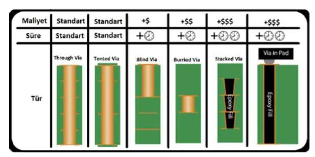
PTH is the most widely used VIA type today. It is the type of hole drilled from the upper layer to the lowest layer. It is the most cost-effective transition hole compared to other VIA types.
Blind VIA
It is a VIA type that starts from the lower or upper layer and completes its connection on any of the intermediate layers.
Buried VIA
It is a VIA type that is used only to make connections between the intermediate layers. In multi layered PCBs, they are embedded in the intermediate layers and cannot be seen from the outside.
Stacked VIA
The advantages of stacked VIAs include not only space savings and increased density but also greater flexibility in terms of internal connections, better routing capacity and less parasitic capacitance. The disadvantage of stacked VIAs, on the other hand, is that are more expensive than standard perforated VIAs or blind/embedded VIAs.
Micro VIA
They are usually transition structures with a small hole diameter placed on the pad. IPC standard definition is a structure with 1:1 hole diameter and depth. Those whose hole diameter difference from the depth does not exceed 0.25 mm are accepted. Micro VIA is an important structure for ensuring the reliability of HDI boards. Blind and Embedded VIAs provide the designers with an advantage in providing much more space and making smaller designs, especially in HDI PCBs. However, when compared to traditional VIAs, the Blind and Embedded VIAs are more difficult to manufacture, and not every PCB manufacturer has this technology.
Types of VIA Protection
VIA Tenting
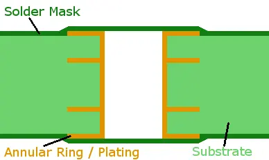
It is the easiest and lowest cost option. On the top and bottom surfaces, the pads of the VIAs are coated with a paint like a tent in order to ensure that the pads of the VIAs do not get soldered and do not come into contact any point and cause a short circuit. If you only delete the solder mask in your data, the VIA will be painted over during manufacturing stage. Also, creating a “Read Me” file in your file and writing “VIAs shall be covered with paint (VIA Tenting)" in the notes section will save you time during the technical approval process.
Conductive Filling: They are usually used in cases with high levels of heating and that require high-flow transport.
Non-Conductive Filling: In this option, VIA is not filled with solder or other contaminants, and in VIA-in-Pad cases, the hole is filled with epoxy instead of air in order to provide structural support. The non-conductive infills have a thermal conductivity of 0.25 W/mK, while the conductive infills have a thermal conductivity between 3.5-15 W/mK. In contrast, electro-plated copper has a thermal conductivity of more than 250W/MK.
Copper-Coated VIA Filled Sample:
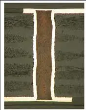
Plugged VIA
It is the coating of both “over” the VIA pads and “inside” the holes with a mask. They are usually preferred for filling VIAs that are very close to BGA pads. They can be produced with much lower costs compared to Filled VIAs.
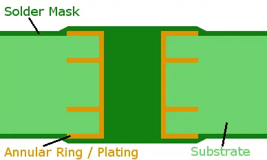
Filled VIAs (Filling with Conductive or Insulating Epoxy)
It is a process that requires high costs in manufacturing.