
R&D AND TECHNICAL SUPPORT ENGINEER
Proteus, developed by Labcenter Electronics, is one of the most intelligent programs in the field of circuit drawing, simulation, animation, printed circuit drawing and 3D modeling. Proteus consists of two parts: ISIS and ARES (Advanced Routing and Editing Software). While making electronic circuit diagram drawings with ISIS, analysis and simulation of these circuits can also be performed. The circuits drawn in ISIS are transferred to ARES, and 3D modeling and printed circuit drawing are performed.
Some of the advantages of the Proteus are;
● Since the electronic circuits can be tested in a simulation environment, time, money and energy are saved.
● Many test equipment can be used in circuits. (Oscilloscope, Signal Generator, etc..)
● Different results can be obtained by easily changing the values of the elements used in the circuit.
● All kinds of processor-based circuits can be tested.
● There is a large library of electronic components.
● The material lists of the drawn circuits can be extracted.
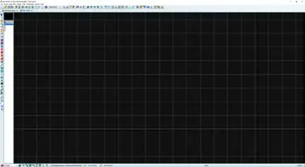
When you launch Proteus, you will see a screen like the one below. Through this screen, you can switch between ISIS and ARES workspaces.

1. Creating a New Project
To create a new project, select “New Project” from the “File” menu in the upper-left corner. The name and folder of the project are determined on the screen that opens. To use Proteus’ ready templates, a selection is made from the “Design Templates” section. The same selection can also be made for the PCB template. If the microprocessor will be used in the project, this processor is selected from the screen and the new project page will be ready.
2. Component Selection
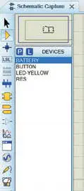
After the project is crated, the component mode is switched to the “Component Mode” via the button on the left menu for the circuit. Then, component selection is made with the “P” button from the tab on the left side.
3. Component Placement and Connection
After the components are selected, they are placed on the project page in order. Then, the connection of these components to each other is made and the schematic of the circuit is created.
4. Circuit Control
If there is any error, missing connection or a component that has been placed in the circuit but not used in the completed circuit, “Electrical Rules Check” is selected from the top menu to check it. The control results related to the circuit are displayed on the page that opens.
5. Simulation
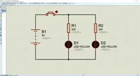
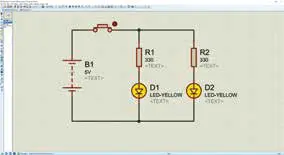
After the electronic circuit is created, a simulation of the circuit can be performed if desired. To start the simulation, the “Run (Play)” button in the lower left section of the project screen is pressed. If there is a microprocessor in the circuit, the software of the microprocessor must be installed before starting the simulation. To do this, right-click on the microprocessor. After clicking on ”Edit Properties“, the software file (.hex) is selected from the ”Program File” section in the window that opens. The operating frequency of the processor can also be changed on this window. After this operation is completed, the simulation is started.
6. Material List (BOM List) Creating
A list can be created very easily in Proteus with the “Bill of Materials” option in the menu above the project. When you click on this option, you can decide which parameters to include in the list, in the window that opens. In the “Generate BOM” tab in the lower left corner, you can select the format that the material list will be saved. It can be saved in HTML, PDF, Excel and CSV formats.
7. Exporting the Circuit Diagram to ARES
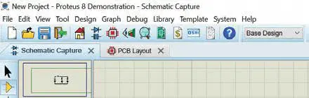
The circuit drawn in ISIS can be exported to ARES, and the PCB drawing stage can be started. To export the circuit to ARES, click on the ARES logo at the top of the project file. After this, a new interface appears on the screen.
8. Layout and Connection of Circuit Elements
After exporting our circuit elements to ARES, the components can be seen in the left menu with “Component Mode”. Before starting to place the components, a graph is selected from the left menu depending on the shape of the PCB that will be created. The graphic is drawn on the project page in desired size. By right-clicking on this shape, the “Board Edge” is performed by changing the layer via the “Change Layer” option. In this way, the boundaries of the PCB will be set. After determining the PCB shape and size, the components are placed on the PCB from the left menu. After the components are placed on the PCB, the connections of the components are formed with the help of the green and yellow guide lines that appear on the components. To make the connections of the components, “Track Mode” is selected in the left menu. After the Track Mode is selected, the path thicknesses that you can choose are displayed on the left tab. Among these options, the appropriate size for the drawing is selected. Component connections are made in this way. After the component connections are also made, “Tools > Power Plan Generator” is selected from the top menu to make a coating path or ground for the circuit. On the display that opens, the connection of the coating, the layer it will be included in, the edge thickness and the distance that the coating can approach other components and PCB edges are selected.
9. Preparation of the Gerber File
After the PCB drawing stage is completed, the stage of preparing the Gerber file for the production of the PCB comes. To create the Gerber file, “Output > Generate Gerber/Excellon File” is selected from the top menu in the ARES interface. In the window that opens, the drawing is continued by clicking on “YES” for pre-testing. If any error is encountered as a result of this test, the system returns to drawing stage, the error is corrected and the same steps are performed again.
If no errors have been encountered, some parameters are set in the window that opens in order to create the Gerber file. Many parameters such as the name of the Gerber file, the folder in which it will be created, and the format in which the file will be output can be changed at this point. After these operations are performed, a Gerber file is created once the “OK” button is clicked. The created Gerber file is reviewed and sent to the manufacturer if no problems have been found.