
RESPONSIBLE FOR PCB ELECTRONIC BOARDS
Gerber is the filing of PCB layers in graphic format. The layout drawing of the PCB design, which is one of the PCB production transition steps, needs to be converted to gerber format. This operation can be done by using the schematic drawing function of design programs (Altium, Proteus, Eagle, Diptrace, Pads, Kicad, Orcad, etc.) or by preparing a printed circuit drawing and exporting it to Gerber format. In addition to design and drawing programs, some CAM programs that control production compatibility by comparing designer tolerances and fabrication limits help in printing production films and verify that the necessary adjustments are made will be required. Some of these programs are CAM350, UcamX, Genesis, Fab3000, Gerbtool, Camtastic and ViewMate. Cam350 is one of the most popular programs on the market. Such programs are a special set of functions that modify, optimize and analyze your PCB design information to ensure quality production by saving time. Now, let’s discuss what is basically being done in Gerber editing program. Import and Export in Several Formats: The design data can be imported from or exported to industry standard formats such as OBB++, IPC2581, Gerber, DXF, Excellon and HPGL.
NC Drill Adjustment
Drills and slots can be modified to the desired sizes, allowing new holes to be easily added to the existing drill table.
CAM Adjustment
Standard modification features such as cut, copy, paste, move, rotate, mirror and trim are available for any element. Allows the user to add flash animations, drawings, lines, polygons and other design elements. Layers can be easily deleted and new layers can be created. Reference indicators, fonts, vias or pad attributes, d-codes, font styles or styles can be changed. These are just some of the features that will allow you to organize your design knowledge.
PCB Panel Design
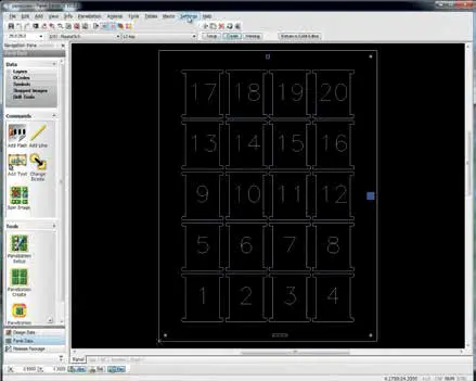
The PCB is paneled in the desired way, using the panel design features. Lath and stamp holes can be added to the desired locations. Since the paneling is done manually, you can automatically prepare the panel distribution with the least material loss, by selecting the automatic panel wizard and entering the basic values. You can produce special panels that contain images from different PCBs, by using the design merging features. You can add mill track and mill tab to determine the CNC points, in order to create a special frame design for the panel. You can export the finished panel design as Gerber, DXF, Mill and Drill, IPC2581 or ODB++ files.
Design Analysis
Using the Design Analysis, the number of layers, card sizes and PCB characteristics such as drill, via technology etc. can be correlated according to the PCB manufacturer’s capabilities. It takes responsibility for the production of designs, without causing excessive costs or delays. It sends the design analysis report to the PCB manufacturer for the cost and delivery estimation of the PCB to be produced. PCB manufacturers can propose design changes that will reduce cost and production time, by considering the report and working together.
Monitoring, Inquiry, Measurement and Reporting
Your design image can be filtered by layers, d-codes, nets, components, drills or spindles. By querying any element by size, shape, area, d-code, design area, drill tool etc. you can get specific details. It also offers the ability to take point-to-point or object-to-object measurements. It allows reporting related to d-codes, bill of materials and netlist information.

Data Conversion and Optimization
You can convert polygons drawn on flash, pad, polygon, line and text drawings to flash, and other drawings to rasterized polygons. It can optimize your design by deleting isolated repetitive pads or copper-coated pads. You can also remove silkscreen ink from the pads.
Flying Probe Adjustment
Using the Flying Probe features, you can determine the bare board test points and fixture placement pin points and provide path controls on the program by assigning test points according to the SMD or TH pad style.
DRC/DFM Analysis
It offers a compliance check of the design rules imposed by the designer for production. By measuring the distance between the lines and the pads, you can check the compatibility with mass production. Also, the minimum and maximum production tolerances such as hole diameters and road thicknesses can be determined. It allows the design to be analyzed for the determination of production obstacle limits and critical design errors. For instance, many errors can be detected, such pad path mismatch (called “acid traps”), pad mask size mismatch, mask-mask distance mismatch, silkscreen presence on the pad and mask, hole being close to the outer section or lines, etc. Also, you can perform advanced analysis in your data for coated or uncoated holes, coppers, blind or embedded vias etc. CAM programs are essential programs required to create and organize PCB production equipment. It is recommended that the CAM specialist make the necessary changes by obtaining the approval from the designer in coordination with the processing of the data.